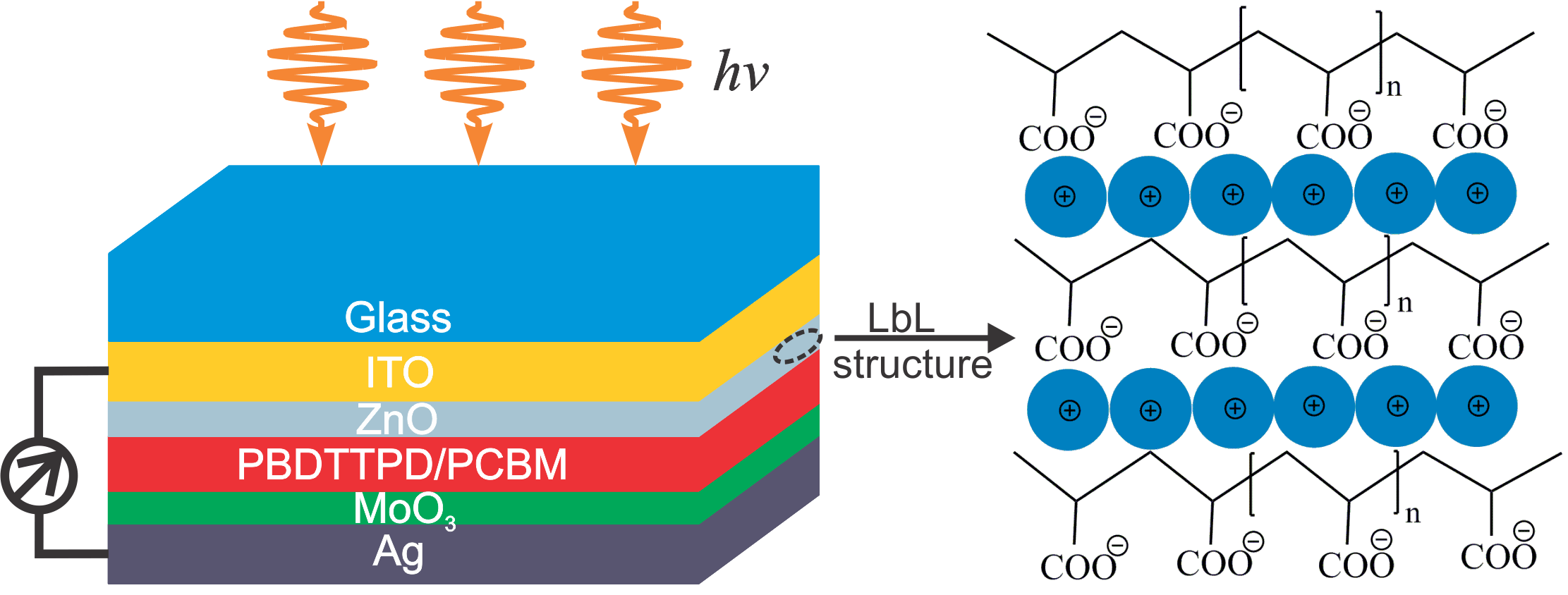
Figure 1: The device architecture of a layer-by-layer ZnO NP/poly(benzo[1,2-b:4,5-b′]dithiophene-thieno[3,4-c]pyrrole-4,6-dione) (PBDTTPD)/[6,6]-phenyl C61 butyric acid methyl ester (PCBM) ordered bulk hetero-junction solar cell. The layer-by-layer structure consisting of multilayers of polyacrylic acid (PAA) and ZnO nanoparticles.
We developed a layer-by-layer (LbL) protocol as a facile, room-temperature, solution-processed method to prepare electron transport layers with a controlled and tunable porous structure, which provides large interfacial contacts with the active layer. Applying this LbL approach to bulk heterojunction polymer solar cells (see Figure 1) yields solar cell power-conversion efficiencies (PCEs) of ca. 6%, exceeding the efficiency of amorphous ZnO interlayers formed by conventional sputtering methods. Our protocol suggests a new fabrication method for solution-processed polymer devices that does not require post-processing thermal annealing treatments and that is applicable to flexible devices printed on plastic substrates.
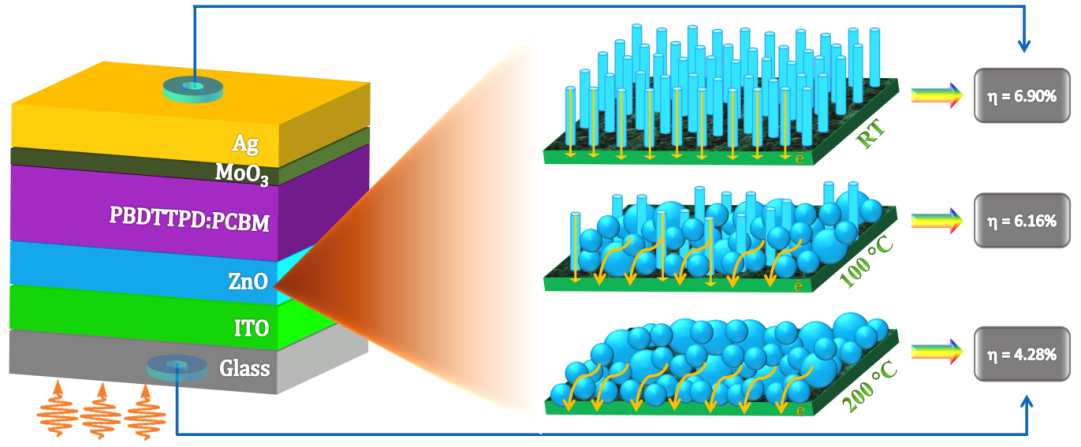
Figure 2: The Impact of Grain Alignment of the Electron Transporting Layer on the Performance of Inverted Bulk Heterojunction Solar Cells.
We have extend this work by reporting a new strategy for improving solar cell PCEs through grain alignment and morphology control of the ZnO electron transport layer (ETL). We show systematic control over the ETL’s grain alignment and thickness via sputtering, by varying the deposition pressure and operating substrate temperature during the deposition. Notably, we demonstrate a high PCE of 6.9%, short circuit current density (Jsc) of 12.8 mA/cm2, open circuit voltage (Voc) of 910 mV and fill factor (FF) of 59% using the PBDTTPD: PCBM polymer blend with ETLs prepared at room temperature exhibiting oriented and aligned rod-like ZnO grains. We show that increasing the deposition temperature during the ZnO sputtering induces morphological cleavage of the rod-like ZnO grains and therefore reduced conductivity from 7.2 ×10⁻¹³ Sm-1 to ~1.7×10⁻¹⁴ Sm-1 and PCE from 6.9 to 4.28% (see Figure 2) when go from RT to 200 degrees. An investigation of the charge carrier dynamics by femtosecond transient absorption spectroscopy with broadband capability reveals clear evidence of faster carrier recombination for a ZnO layer deposited at higher temperature, which is consistent with the trends observed in the conductivity and device performance. Finally, the advantage of the room temperature processed uniform, smooth ZnO films (rms roughness ≤ 2 nm) is that they can be used for flexible transparent solar cells. This method is expected to be applicable to any inverted polymer-fullerene bulk heterojunction (BHJ) device, as well as to other solar cell device architectures.
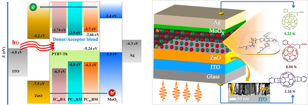
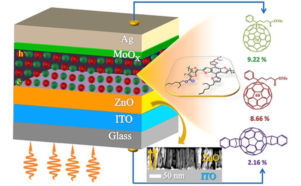
Figure 3: Schematic energy level diagram of the complete solar cell used in this study (left panel). The device architecture, cross sectional scanning electron microscope image of the ZnO hole transporting layer, chemical structure of the donor and the three molecular acceptors and the device efficiency (right panel).
We have tested the impact of grain alignment and morphology control of the ZnO electron transport layer on other photoactive material using similar device architecture and different molecular acceptors. More specifically, Here, we examine results from time-resolved laser spectroscopy and high resolution electron microscopy to provide the fundamental information necessary to fabricate and optimize organic solar cell devices. In real time, we monitor CT and charge separation (CS) at the interface between three fullerene acceptors (FAs) (PC71BM, PC61BM, and IC60BA) and the PTB7-Th donor polymer. Femtosecond transient absorption (fs-TA) data demonstrates that photo-induced electron transfer from the PTB7-Th polymer to each FA occurs on the sub-picosecond time scale, leading to the formation of long-lived radical ions. We also found that the power conversion efficiency improves from 2% in IC60BA-based solar cells to > 9% in PC71BM-based devices, in support of our time-resolved results and the energy level alignment between donor and the three molecular acceptors (see Figure 3). The insights reported in this manuscript provide a clear understanding of the key variables involved at the device interface, paving the way for the exploitation of efficient CS and subsequently improving the photo conversion efficiency. Moreover, these results demonstrate clearly that time-resolved laser spectroscopy and high-resolution electron microscopy can illustrate the basis for fabricating solar cell devices toward optimization.