In the field of photovoltaics, ultrafast interfacial charge transfer (CT), charge separation (CS), charge recombination (CR), and transport are among the key factors in determining the overall efficiency of a solar cell. In this regime, precise knowledge of the mechanisms of these processes on the nanometer (nm) and femtosecond (fs) scales is still urgently required to address various fundamental questions related to the performance of solar cells and many other optoelectronic devices. Since the accessibility of surface dynamics with high spatial and temporal control over a spontaneous photo-induced reaction is a particularly challenging task with many potential breakthroughs in various fields of research of significance including interfacial chemistry, photo-catalysis and solar cells, we have established and developed the second generation of four-dimensional (4D) scanning ultrafast electron microscopy (S-UEM) and demonstrate the ability to record time-resolved images (snapshots) of material surfaces with 650 fs and ~ 5 nm temporal and spatial resolutions, respectively. In this method, the surface of a specimen is excited by a clocking optical pulse and imaged using a pulsed primary electron beam as a probe pulse, generating secondary electrons (SEs), which are emitted from the surface of the specimen in a manner that is extremely sensitive to the local electron/hole density, providing direct and controllable dynamical information about the localization of electrons and holes near interfaces and heterojunctions (Figure 1), which cannot be accessed by any static electron imaging and time-resolved laser spectroscopic techniques.
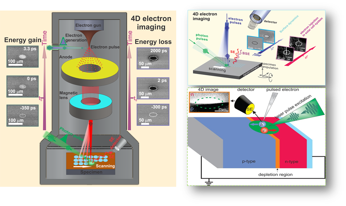
Figure 1: A conceptual schematic of S-UEM where the interface of an fs laser system to a modified SEM (left panel). The probing electron pulses can be adjusted with respect to that of an optical initiating pulse (right upper panel), mapping surface dynamics at p-n type interface following fs optical excitation (right, lower panel).
The concept of S-UEM is entirely unique in that nanometer spatial resolution is that of a conventional SEM and the fs time resolution is determined by the ultrashort laser pulses involved, not by the conventional deflection rate or the streak camera used for optical detection. Our S-UEM experimental design is comprised of a fs Clark-MXR fiber laser operating at a central wavelength of 1030 nm with a pulse width of 270 fs integrated with a modified FEI Quanta-650 SEM (Figure 2). The fundamental laser output is divided by a beam splitter and directed to two independent harmonic generators (HGs) to produce the second and third harmonic signals at 515 and 343 nm, respectively. The output of the first HG (343 or 515 nm) is directed with precision through a pyrometric quartz window and is tightly focused on a field-emitter tip to generate the pulsed electrons for imaging. The output of the second HG (515 nm, excitation clocking pulse) enters the microscope at an angle of 50° relative to the surface normal and is focused onto the specimen surface to initiate the dynamics. Finally, a computer-controlled optical delay line is used to vary the timing between the electron and photon pulses. Upon illumination of the specimen with the pulsed photoelectrons, SEs are emitted from the sample surface and detected by a positively biased Everhart-Thornley detector. All experiments were conducted at a laser repetition rate of 2–8 MHz to ensure full relaxation of the material dynamics to its equilibrium state prior to the arrival of the subsequent excitation pulse. To enhance the signal-to-noise ratio, the SE images were obtained as an integration of 64 frames with a dwell time of 300 ns at each pixel.
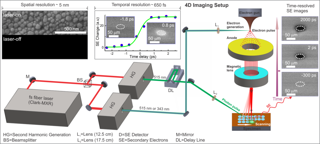
Figure 2: Schematic of the experimental setup with the femtosecond laser integrated with SEM. The left inset shows an image of Au nanoparticles in the presence and absence of the photoelectron-generating laser pulse. The right inset shows the characterization of the instrument’s temporal resolution obtained by fitting the change in contrast for time-resolved difference images of a CdSe single crystal.
To determine the spatial resolution of our setup, gold nanoparticles were imaged using pulsed photoelectrons generated by the laser pulse from the field emission gun (Figure 2). High-quality images were obtained that provided a spatial resolution of approximately
5 nm. The same image has been taken in the absence of laser irradiation. In this case, a negligible background originating from the thermal electrons is observed, thus confirming the use of pulsed photoelectrons to construct the images. The temporal
resolution of the instrument was determined by fitting the time-dependent intensity change of the SEs to an error function. In this manner, a temporal resolution of 650 fs was obtained.
Here, we highlight the capabilities of S-UEM. The pump-probe scheme employed in S-UEM offers an interesting scenario in terms of probing dynamical processes on material surfaces in space and time. As shown in Figure 3, in addition to the
commonly used photon-electron dynamical probing, where a clocking optical pulse arrives first to initiate dynamics and is probed by pulsed electrons, there is another regime of probing (referred to as electron-photon dynamical probing) when the electron
pulse arrives before the clocking pulse near t0. Such an observation in the regime of electron-photon dynamical probing is only possible if the later-arriving photons, which can be as late as >100 ps, cause a change in the non-instantaneous SE
emission, providing a unique means to study the dynamics of SE emission on material surfaces in space and time.
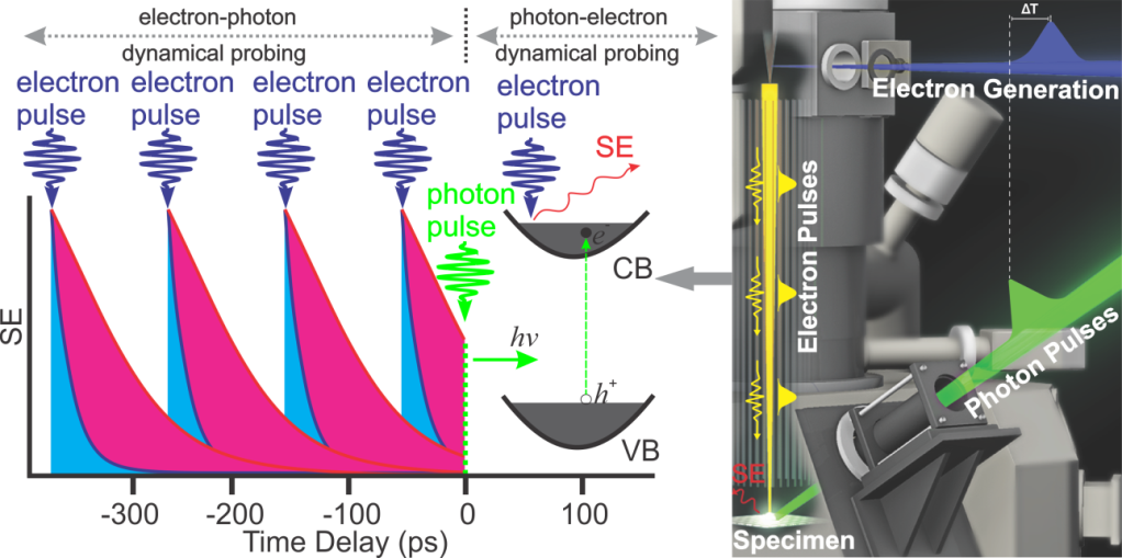
Figure 3: Schematic of the dynamical information obtained in the electron-photon and photon-electron dynamical probing regimes.
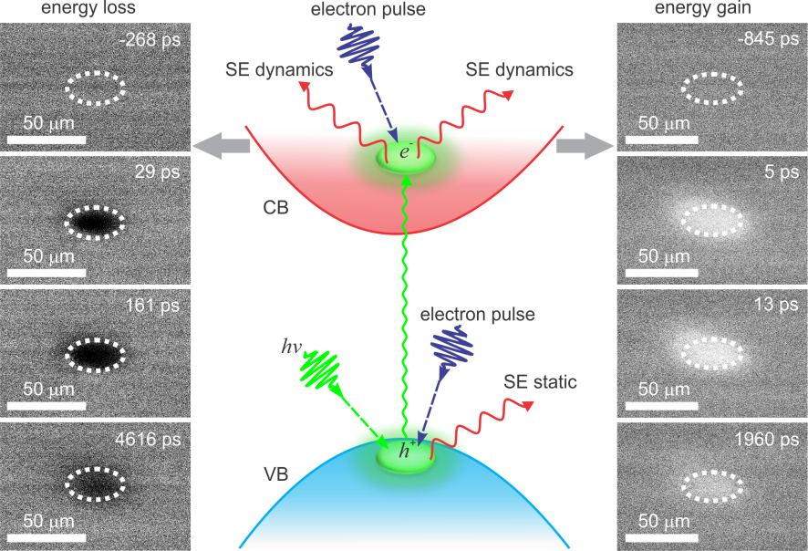
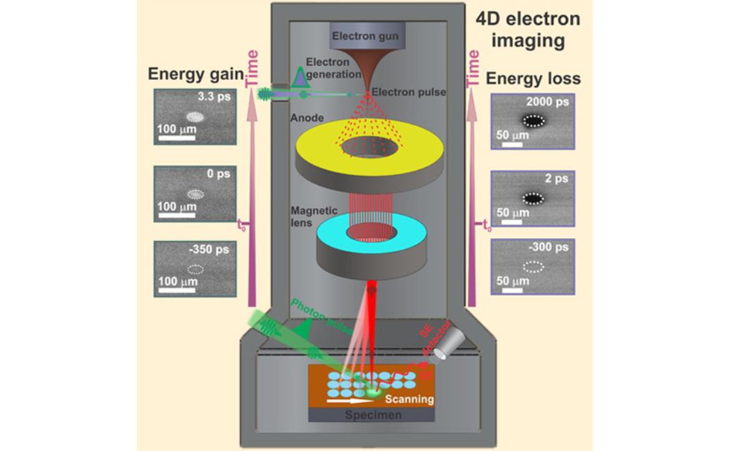
Figure 4: Mechanisms for the dynamics observed in S-UEM, where the valence band electrons are promoted to the conduction band upon optical excitation. The dashed ellipse indicates the location of the laser on the specimen. Several time-resolved images at selected times are displayed to indicate the contrast development. High contrast (right panel) is recorded because of the energy gain, and dark contrast (left panel) is recorded because of the energy loss at the center of the excited region.
Interestingly, bright or dark contrast change can be observed in S-UEM experiments. Generally, an inter-band carrier transition occurs when the clocking optical pulse excites the surface of the specimen and a fraction of the valence-band electrons are
promoted to the conduction band (Figure 4, middle panel). Consequently, in contrast to an unperturbed specimen, the promoted electrons have a higher probability of emitting SEs above the vacuum level when scattered by the energetic primary electron
beam, resulting in an enhancement (“SE energy gain”) (Figure 4, right panel) of the image contrast, which appears as a bright contrast in the difference images. In contrast, the appearance of dark contrast at positive delay times in different
semiconductor materials, including InGaN nanowires and CIGS quantum dots, can be observed, indicating a suppression of the emitted SEs through scattering processes (“SE energy loss”) (Figure 4, left panel). In other words, the dark contrast
observed in some cases suggests a different mechanism in which the SEs in the conduction band lose their energy while travelling to the surface to come out. In this case, scattering processes with photo-generated electron-hole pairs are likely responsible
for the energy loss. Because the effective cross-section for the scattering of SEs with conduction band electrons is considerably higher than that with valence electrons, a decrease in SE emission and thus a low contrast is observed.
In several unique applications, we can now spatially and temporally visualize the SE energy gain and loss, the charge carrier dynamics in semiconductors materials including diffusion on the surface of InGaN nanowires, quantum dots and
CdSe single crystals.