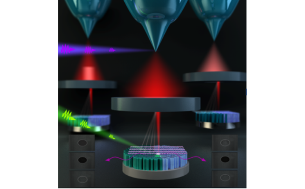
In this work, we spatially and temporally visualize the charge carrier dynamics on the surface of InGaN NW arrays before and after surface passivation with octadecylthiol (ODT) using S-UEM (Figure 1 left panel). The time-resolved SE images clearly demonstrate that carrier recombination on the NW surface is significantly slowed down after ODT treatment (Figure 1, right panel), providing clear evidence of the minimization of the surface defects. This observation is fully supported by elemental mapping of the NWs which shows removal of surface oxygen along with formation of carbon rich amorphous layer on the surface of NWs after ODT treatment and enhancement of the performance of the light emitting device. Direct observation of surface dynamics provides a profound understanding of the photo-physical mechanisms on materials’ surfaces and enables the formulation of effective surface trap states management strategies for the next generation of high performance NW based optoelectronic devices.
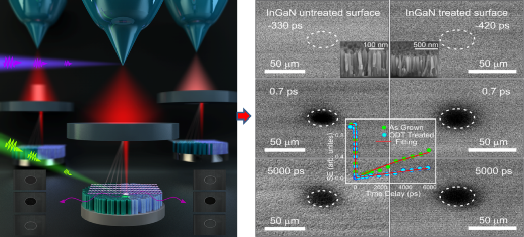
Figure 1: Schematic representation of our experimental setup for mapping InGaN NWs before and after surface treatment (left panel). Time-resolved SE difference images exhibiting the contrast evolution in InGaN nanowires before (left) and after (right) ODT passivation at selected time delays. The insets in the two topmost images depict the cross-sectional SEM images. The middle inset shows the kinetic traces of the change in contrast (fitted to exponentials) in both the samples as a function of the time delays.