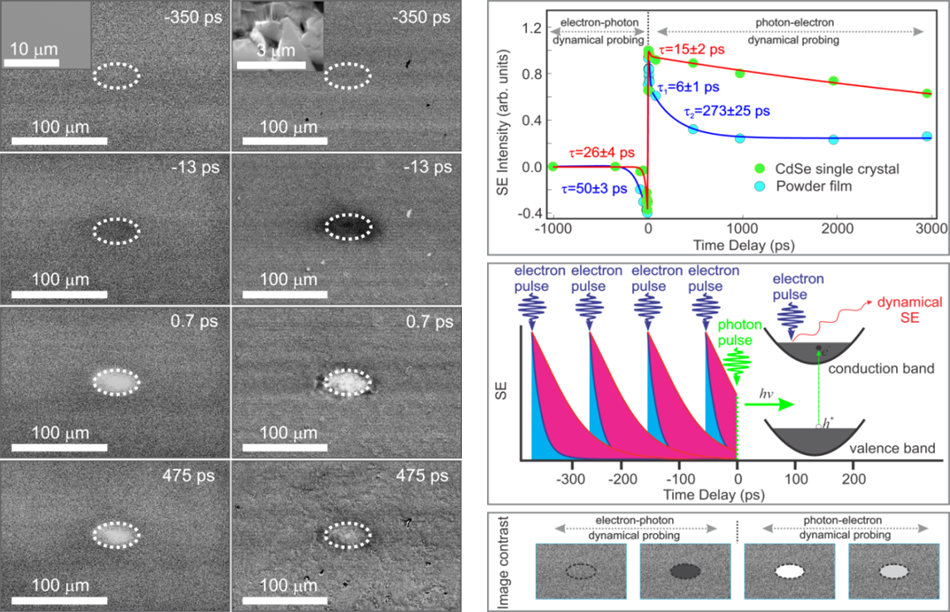
By visualizing different surface of CdSe single crystals, we show that the morphology, grains and nanostructure features of the material surface can impact the overall carrier relaxation processes. To confirm that the morphology, grains and surface defects are key components for controlling the carrier dynamics on materials surfaces, we conducted time-resolved imaging on a crystalline powder film made by mechanical grinding of a CdSe single crystal (Figure 1, left panel). A fast recovery of the bright contrast is observed (Figure 1, right panel) due to charge carrier recombination, with characteristic time constants of 6 and 273 ps. The two time constants can be attributed to different scattering sources i.e., grains, structured features and defects and thus serve as surface trapping centers to remove a substantial portion of the excited carriers that create bright contrast. This surface information cannot be selectively obtained by any time-resolved laser spectroscopic techniques because they are limited by the laser’s relatively large penetration depth, and therefore these techniques record mainly bulk information.

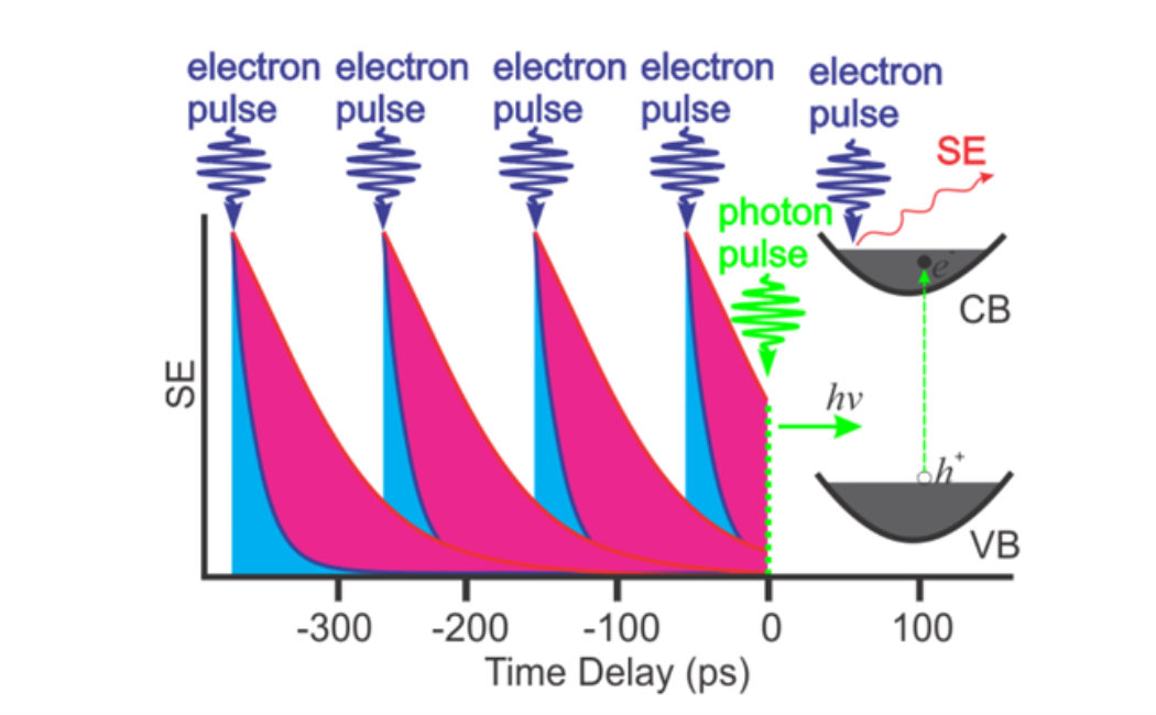
Figure 1: Time-resolved difference images of CdSe single crystals and its crystalline powder film at selected delay times (left panel). The dashed ellipses indicate the footprint of the clocking optical beam on the specimen. Scanning electron micrographs of the single crystal and the crystalline powder film is shown in the Inset. Dynamics of SE intensities obtained from the center of the excited region for CdSe single crystal (red) and its powder film (green). Middle panel shows the schematic for the information on dynamics obtained in the CdSe single crystals and powder films, in the regimes of electron-photon and photon-electron dynamical probing. Shown in the lower panel are contrast change in the images of the CdSe single crystal and its powder film in the two regimes of probing.