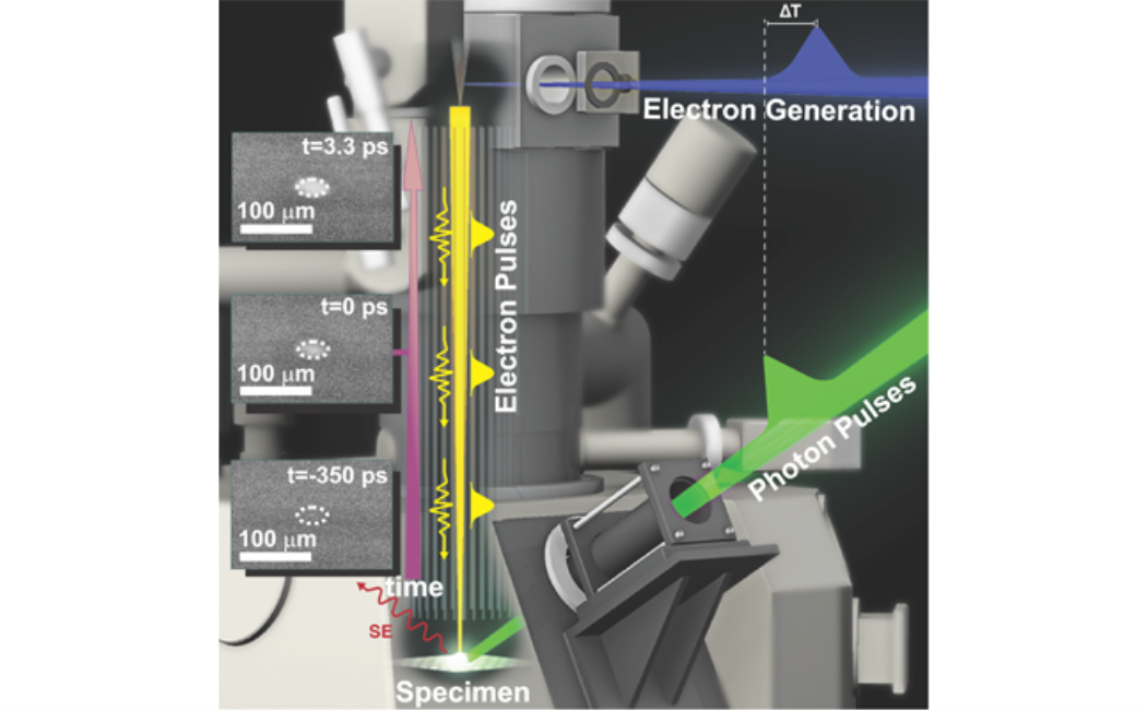
Figure 1: Schematic presentation of our S-UEM setup (right) and SE images show the carrier spreading on the surface of a densely packed array of InGaN nanowires.
Using our S-UEM with a 650 fs and ~5 nm temporal and spatial resolutions, respectively, we show that time resolved imaging of the energy loss dynamics and carrier spreading on the surfaces of a densely packed array of InGaN nanowires (NWs) as a model system can be achieved now in real space (Figure 1), providing direct and depth-selective information regarding surface dynamics which could not be accessed otherwise. Significantly, we modelled the variation in SE signal in time and space to extract fundamental materials parameters that describe carrier relaxation and diffusion processes in these nanomaterials. Moreover, we identified the possible deactivation channels and the mechanism of SEs energy loss in the system, which will help unlock the full potential of this material for various applications especially in optoelectronic devices.